

News and Information
Glass substrate, turning point
Glass substrate, turning point
Release time:
2023-07-08
Source:
Reprinted from 36Kr
Author:
Semiconductor Industry Watch
In 2022, SKC’s U.S. subsidiary, Absolics, invested approximately KRW 300 billion (about USD 222 million) to establish its first factory in Covington, Georgia, U.S., specializing in the production of glass substrates. Recently, the company announced that the factory has been completed and has begun mass production of prototype products, marking a turning point for the rapidly growing glass substrate market.
In 2022, SKC’s U.S. subsidiary, Absolics, invested approximately KRW 300 billion (about USD 222 million) to establish its first-ever factory specializing in the production of glass substrates in Covington, Georgia, USA. Recently, the company announced that the factory has been completed and has begun mass production of prototype products, marking a turning point for the rapidly growing glass substrate market.
The glass substrate market is witnessing fierce competition among key players such as SKC, Samsung Electro-Mechanics, and LG Innotek. Glass substrates are highly valued for their ability to process large volumes of data rapidly and for their superior energy efficiency compared to traditional plastic substrates. Although this technology is still in its early stages, according to The Insight Partners, the global market size is projected to grow from $23 million this year to an impressive $4.2 billion by 2034.
Currently, the plastic-substrate market is dominated by Japan’s Ibiden and Kanzo Electric, as well as Taiwan’s Unimicron. However, as the demand for semiconductor performance in the field of artificial intelligence continues to rise, the shift toward glass substrates represents a significant technological advancement.
Why are glass substrates needed?
In the advanced packaging industry, with the emergence of glass core substrates, the innovation race has reached a new critical juncture.
This new technological direction has emerged following the wave of organic and ceramic substrates and holds promise for overcoming the challenges associated with organic core substrates. By boosting performance, efficiency, and scalability to new levels in terms of chip design and manufacturing costs, it aligns with the broader trends in HPC and AI. The success of this approach, however, hinges on the maturity of the technology and its widespread adoption in end markets.

As a material, glass has been extensively studied and integrated into numerous semiconductor industries. It represents a significant advancement in the selection of advanced packaging materials and offers several advantages over organic and ceramic materials. Unlike organic substrates, which have long been the mainstream technology, glass boasts exceptional dimensional stability, thermal conductivity, and electrical performance.
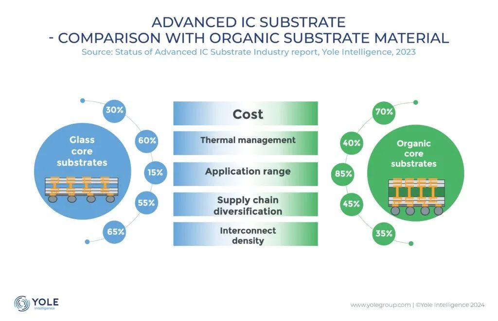
However, despite its potential benefits, like any new technology, glass-core substrates also face a series of challenges—not only for substrate manufacturers but also for suppliers of equipment, materials, and testing tools.
Despite these challenges, the adoption of glass-based substrates continues to be driven by several key factors. The growing demand for larger substrates and more compact form factors, coupled with the technological trends toward chip and heterogeneous integration, are prompting the industry to consider glass as a promising solution. Moreover, once this technology matures and gains widespread adoption, the potential cost advantages of glass will make it an attractive option for the high-performance computing (HPC) and data center markets.
In this field, through-glass vias (TGVs) are one of the key pillars of glass-core substrates. TGVs pave the way for more compact and higher-performance devices. They help increase the density of interlayer connections. These vias also contribute to improving signal integrity in high-speed circuits. By reducing the spacing between connections, TGVs minimize signal loss and interference, thereby enhancing overall system performance. The integration of TGVs can simplify manufacturing processes by eliminating the need for separate interconnect layers. However, despite their numerous advantages, TGVs also face several challenges. Due to the complexity of the manufacturing process, TGVs are more prone to defects that could lead to product failures. Moreover, TGVs typically entail higher production costs compared to other solutions. The demand for specialized equipment, combined with the risk of defects, can further drive up manufacturing expenses. Recently, many new patents related to TGVs have been granted to laser equipment manufacturers such as LPKF. These advancements are helping to accelerate the commercialization of glass-core substrates while addressing the challenges associated with glass interposers. This solution enhances both GCS and glass interposers, holding great promise for the development of exciting next-generation high-performance devices.
In addition, the synergy between glass-based substrates and panel-level packaging (PLP) is driving innovation in both fields. Since both technologies utilize similar panel sizes, they offer complementary opportunities for increasing chip density, reducing costs, and enhancing manufacturing efficiency.
Glass-based substrates represent a promising frontier in the fields of advanced IC substrates and advanced packaging. They offer unparalleled performance and scalability for next-generation chip design and packaging. Although challenges remain—just as with any new technology—collaborative efforts by industry leaders and new entrants are paving the way for the widespread adoption of glass-based substrates across various end markets, with AI chips and servers emerging as key drivers. As GCS technology matures and supply-chain infrastructure continues to develop, glass-based substrates hold great potential to redefine the landscape of advanced packaging.
The Big Players' Strategies
Last September, Intel launched a new glass-substrate technology for system-in-package chips based on large-scale chips, kicking off the race to develop glass substrates.
Any engineer knows that ICs are more than just silicon. Various components—such as packaging, leads, and substrates—play a critical role in determining the durability and overall performance of a component. Among these, the substrate—the material on which the silicon IC die is mounted—has become increasingly important in enabling higher computing power within a single package. To meet these growing demands, Intel has announced the launch of a new glass-substrate technology designed for next-generation high-power processors.
Babak Sabi, Intel’s Senior Vice President and General Manager of Assembly and Test Development, stated: “After a decade of research, Intel has achieved industry-leading advanced packaging glass substrates. We look forward to rolling out these cutting-edge technologies, enabling our key partners and foundry customers to reap benefits for decades to come.”
According to Intel, glass boasts unique properties compared to today’s organic substrates—such as ultra-low surface flatness and superior thermal and mechanical stability—thereby significantly boosting interconnect density within the substrate. These advantages will enable chip architects to create high-density, high-performance chip packages tailored for data-intensive workloads like artificial intelligence (AI). Intel expects to bring a complete glass-substrate solution to the market in the second half of this century, enabling the industry to continue advancing Moore’s Law beyond 2030.
Intel believes that by the end of this century, the semiconductor industry may reach its limits—specifically, the use of organic materials to shrink transistors on silicon packaging. This approach would consume more power and face limitations such as shrinkage and warping. Shrinking transistors is crucial for the advancement and development of the semiconductor industry, and glass substrates represent a viable and essential next step toward the next generation of semiconductors.
As the demand for more powerful computing capabilities continues to grow and the semiconductor industry enters a heterogeneous era characterized by multi-chip packaging, improvements in signal transmission speed, power delivery, design rules, and package substrate stability will become critically important. Compared to the organic substrates currently in use, glass substrates offer superior mechanical, physical, and optical properties, enabling the integration of more transistors within a single package, providing better scalability, and allowing the assembly of larger chip complexes—known as “system-in-package” solutions. Chip architects will be able to pack more chips (also referred to as die) into a smaller footprint within a single package, while simultaneously achieving higher performance and density, greater design flexibility, and reduced overall cost and power consumption.
From Intel’s perspective, glass substrates will first be introduced into markets that can make the most of their advantages—applications and workloads that demand larger form factors (such as data centers, artificial intelligence, and graphics) and higher-speed capabilities.
Glass substrates can withstand higher temperatures, reduce pattern distortion by 50%, exhibit ultra-low flatness, improve the depth of focus in lithography, and provide the dimensional stability required for extremely tight interlayer interconnects. Thanks to these unique characteristics, the interconnect density on glass substrates can be increased by a factor of 10. Moreover, the mechanical properties of glass have been enhanced, enabling the realization of ultra-large-size packages and delivering exceptionally high assembly yields.
The glass substrate’s tolerance to high temperatures also provides chip architects with greater flexibility, enabling them to set design rules for power delivery and signal routing more freely. This is because the substrate allows for seamless integration of optical interconnects and enables inductors and capacitors to be embedded directly into the glass during high-temperature processing. As a result, it becomes possible to develop superior power delivery solutions while simultaneously achieving high-speed signal transmission at low power levels. These numerous advantages bring the industry closer to its goal of scaling up packaging to accommodate 1 trillion transistors by 2030.
As a key player in the industry, Samsung doesn't want to be left behind.
According to a March report by the foreign media outlet Sedaily, as one of the world’s largest chip manufacturers, Samsung naturally wouldn’t overlook glass substrates. Therefore, the company recently established an alliance composed of its own teams, aiming to research, develop, and commercialize glass substrates by 2026.
Samsung has formed an alliance comprising Samsung Electro-Mechanics, Samsung Electronics, and Samsung Display to develop and commercialize glass substrates in the shortest possible time. In fact, as early as CES, Samsung Electro-Mechanics announced its plan to begin mass production of glass substrates by 2026.
An industry insider told Sedaily: “Since each company possesses the world’s most advanced technology in its respective market, synergies will be maximized in the promising field of glass-substrate research. At the same time, it’s important to pay attention to how Samsung’s alliance will build its glass-substrate ecosystem.”
Samsung Electronics is expected to focus on the integration of semiconductors and substrates, while Samsung Display will concentrate on glass processing. This collaborative approach is designed to strengthen the group’s competitive edge.
Subsequently, in May, the foreign media outlet ETNews reported that Samsung Electro-Mechanics is accelerating its entry into the semiconductor glass substrate market. The company has advanced the procurement and installation of equipment to September and plans to start operating a pilot production line in the fourth quarter—earlier by one quarter than originally scheduled. The company expects to begin mass production of glass substrates for high-end system-in-package (SiP) applications in 2026. To secure orders for 2026, the company needs to demonstrate strong capabilities in 2025.
To build highly complex multi-chip SiPs, Samsung needs to acquire expertise in glass substrates. Therefore, the company decided to advance the timeline for its pilot production line at the Sejong plant in South Korea—a strategic move that likely reflects the growing importance of advanced chip packaging technologies for Samsung and the company’s proactive efforts to wrest market share from Intel, which is expected to begin offering advanced glass-substrate packaging in the coming years.
According to reports, Samsung Electro-Mechanics plans to install all necessary equipment on the pilot production line by September and begin operations in the fourth quarter.
The selection of suppliers has been completed, and companies such as Philoptics, Chemtronics, Joongwoo M-Tech, and Germany’s LPKF are responsible for providing components for this device. According to reports, the device is designed to streamline production and comply with Samsung’s stringent safety and automation standards.
As Samsung’s foundry seeks to secure more orders from data-center-grade processor developers, the company will also need to offer advanced packaging services. To this end, Samsung Electro-Mechanics’ (and indeed, Samsung as a whole) efforts related to glass substrates could soon become critical to Samsung’s foundry business.
LG Innotek has also entered the development of glass substrates. LG Innotek’s core R&D division, the CTO Department, recently began recruiting personnel to develop semiconductor glass substrates. Earlier, LG Innotek CEO Hyuk-soo Moon stated at the company’s shareholders’ meeting in March, “Large U.S. semiconductor companies are showing interest in glass substrates,” and “LG Innotek is also preparing for the glass substrate business.”
Moreover, the emergence of new companies such as SCHMID, along with the participation of laser equipment suppliers, display manufacturers, chemical suppliers, and others, highlights the diversified ecosystem taking shape around the nascent supply chain for glass-substrate substrates. All parties are forging collaborations and partnerships to address the technical and logistical challenges associated with glass-substrate manufacturing, demonstrating a collective effort to fully unlock the potential of this emerging field.
Written at the end
While major manufacturers are vigorously promoting the adoption of glass substrates, downstream customers have also expressed strong enthusiasm for their use. Intel, of course, is a prime example; other companies such as NVIDIA, AMD, and Apple are also seen as potential “buyers” of glass substrates.
However, despite its many advantages, there are still numerous factors that need to be addressed before glass substrates can be fully commercialized. The biggest challenge is their fragility. The industry believes that it will take some time before mass production yields reach a level sufficient for practical delivery. Moreover, the company’s upfront investment costs are extremely high. Even if a company makes substantial investments in technological development, these costs will become sunk costs if the business fails to turn a profit.
Ko Eui-young, a researcher at Hl Investment & Securities, said: “The glass substrate requires a restructuring of the supply chain because equipment needs to be replaced, and further verification of the reliability associated with glass materials is necessary.” “Standardizing mass production is essential, but the yield rate during mass production remains uncertain.” However, from a long-term perspective, the industry generally agrees that glass substrates should be developed.
Lee Kyu-ha, a researcher at NH Investment & Securities, stated: “To optimize the trend of semiconductor miniaturization, glass will become the core substrate material of the future.”