

News and Information
Glass chips are set to take off—thanks to AI.
Glass chips are set to take off—thanks to AI.
Release time:
2023-06-26
Source:
Reprinted from 36Kr
Author:
Lei Technology
As the biggest “shovel seller” in this wave of AI, NVIDIA continues to forge ahead at a rapid pace. Its recently released financial report shows that the company’s revenue for the latest quarter has surged to 3.6 times its level from the same period last year. It’s no wonder, then, that every move NVIDIA makes draws intense attention.
As the biggest “shovel seller” in this wave of AI, NVIDIA continues to forge ahead at a rapid pace. Its recently released financial report shows that the company’s revenue for the latest quarter has surged to 3.6 times its level from the same period last year. No wonder then that every move NVIDIA makes draws intense attention.
A few days ago, the international investment bank Morgan Stanley released a report indicating that NVIDIA’s GB200 superchip (CPU+GPU), based on the latest Blackwell architecture, will use glass substrates rather than the more common organic substrates. This has drawn even greater attention to “glass substrates” and “glass chips.”
But in reality, NVIDIA isn't the only company that might use glass substrates for chips—companies including Intel, Samsung, and Apple are also openly or subtly optimistic about the arrival of “glass chips.”
Amid the ongoing surge in demand for AI, Intel was the first to launch glass substrates for next-generation advanced packaging last year and announced that it will roll out complete solutions in the coming years. The first batch of chips based on glass substrates will target data centers and AI high-performance computing applications.
Samsung plans to be even more aggressive: As early as early May of this year, it announced that it expects to begin mass production of glass-based substrates for high-end System-in-Package (SiP) solutions by 2026. According to reports, Samsung intends to complete the procurement and installation of all necessary equipment by September and start operating a pre-commercial production line in the fourth quarter of this year.
So, what exactly is a glass substrate? Why are chip giants racing to catch the AI wave all focusing on glass substrates? And what value can glass-based chips—glass chips—bring to computing devices and ordinary users?
What is a glass chip?
Computing power can be said to be one of the terms most frequently mentioned in the AI boom over the past year or so. In fact, even before this current wave of AI, stronger computing demands and more sophisticated semiconductor circuits have already placed higher requirements—not only on chip packaging processes but also on everything from substrate materials down to the smallest components.
Readers familiar with chip manufacturing may know that the diced chips—also known as bare dies—cannot be called “chips” until they’ve been packaged. Packaging not only enables the chip to establish electrical and signal connections with the external environment but also provides the chip with a stable operating environment.
In this process, organic materials are typically used as substrates to encapsulate chips; the essence of glass-based chips is simply replacing the organic substrate with a glass substrate. However, compared to their organic-substrate counterparts, glass-based chips offer superior electrical performance, enhanced high-temperature resistance, and larger package sizes.
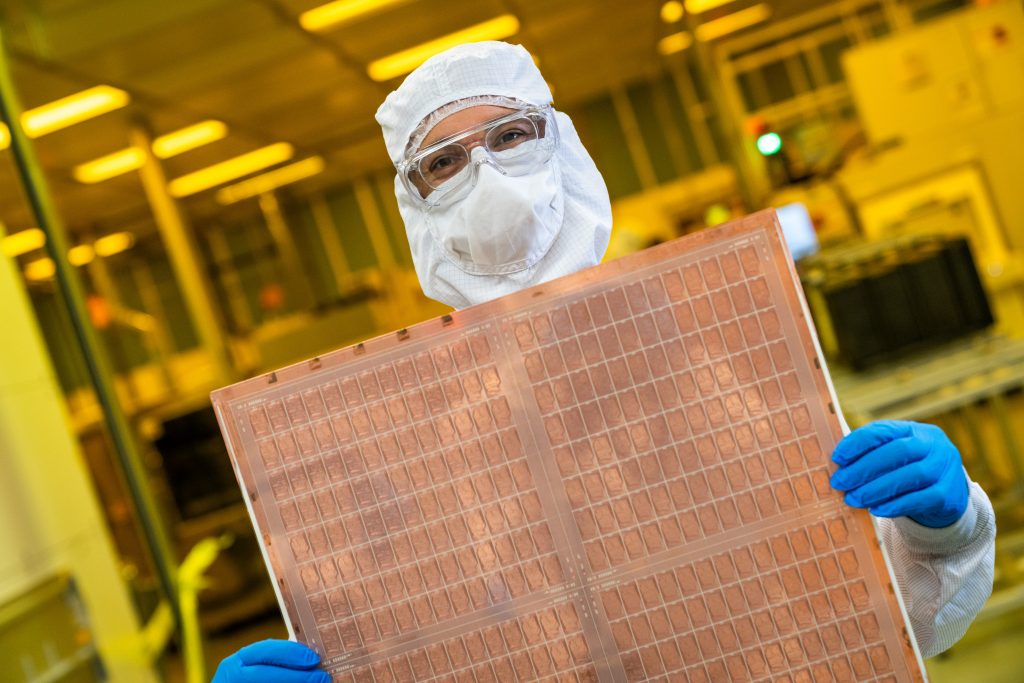
Glass substrate, photo/Intel
Superior electrical performance means that glass substrates can enable clearer signal and power transmission. Intel points out that glass substrates can support signal transmission rates of up to 448 Gbps, achieving lower signal loss. And lower signal loss also means that glass substrates can help chips become more energy-efficient.
Moreover, unlike the rough surfaces of organic plastics, the smoother glass substrate makes photolithography and packaging easier, allowing for a greater number of openings per unit area.
Also due to their physical properties, glass substrates offer superior thermal and mechanical stability. As a result, during the operation of high-performance computing chips that generate substantial heat, these chips are less likely to warp or deform. After introducing TGV (Through-Glass Via) technology, Intel will be able to reduce the spacing between vias to less than 100 micrometers, directly increasing interconnect density between chips by a factor of 10.
However, the above-mentioned points may not be the most important ones yet. Compared to organic substrates, glass substrates allow for larger chip package sizes, enabling the integration of more and larger dies—and thus, more transistors. According to Intel, they can fit 50% more dies onto glass substrates, significantly boosting packaging density.
Therefore, whether in terms of performance, power consumption, or interconnect density, glass substrates—or, more precisely, glass chips—are the superior choice. From this perspective, it’s hardly surprising at all that NVIDIA’s GB200 would indeed adopt glass substrates.
The battle for computing power is spreading like wildfire.
As Moore’s Law continues to approach physical limits, it has become increasingly difficult to substantially improve the performance of a single die. At the same time, however, the demand for high computing performance is growing ever more urgent. Chiplet technology—small chips—has now been widely recognized as one of the primary approaches for boosting chip computing power in the future.
In March of this year, NVIDIA unveiled the next-generation Blackwell GPU architecture—and the GB200 superchip built on this architecture—at the GTC developer conference. The GB200 marks NVIDIA’s formal entry into the chiplet era. Each GB200 actually comprises two B200 GPUs and one Grace CPU, with each B200 GPU containing 208 billion transistors.
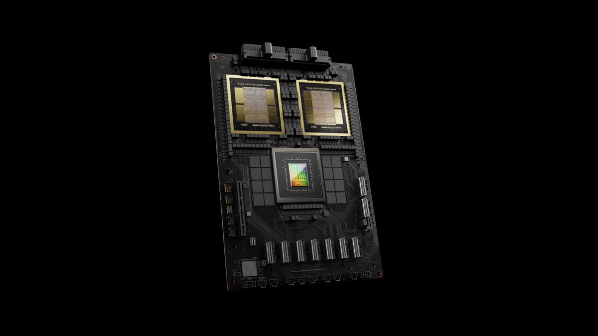
GB200, Image/NVIDIA
Moreover, compared to the previous-generation H100, which required 8,000 Hopper GPUs and 15 megawatts of power to train a 1.8-trillion-parameter model, this new-generation B200 can accomplish the same task using just 2,000 Blackwell GPUs and 4 megawatts of power.
Simply put, chiplet technology involves integrating multiple dies—or small chips—into a single package. To put it more colloquially, it’s like using “glue” to connect several small chips together, creating a more powerful chip. Examples include NVIDIA’s GB200 and Apple’s M2 Ultra.
However, the trend toward chiplets has also placed new demands on substrate signal transmission speed, power delivery capability, design, and stability. Yet, due to their physical limitations, organic substrates are becoming increasingly inadequate—and this is precisely one of the key reasons why glass substrates are receiving growing attention.
On the other hand, this is also driven by competition in the advanced packaging technology sector.
Currently, TSMC’s CoWoS packaging technology is unrivaled worldwide and boasts high technological and patent barriers. At the market level, thanks to its CoWoS packaging technology, TSMC has essentially captured the majority of AI chip orders from leading chip design companies—from NVIDIA to AMD, from Google to Microsoft.
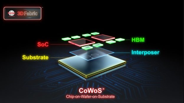
CoWoS, Image/TSMC
As competitors, Intel and Samsung clearly won't be willing to accept their current position. However, beyond stepping up their efforts to catch up with TSMC's packaging technologies along similar technological paths, Intel and Samsung may also realize that it will be extremely difficult for them to surpass TSMC on this front. In contrast, glass substrates might represent a genuine opportunity to outpace TSMC in the field of packaging technology.
Therefore, it’s not hard to understand why, starting last year, both Intel and Samsung—two major wafer foundries—have been stepping up their investments in glass substrates, accelerating plans to ramp up mass production of glass-based chips. Indeed, according to industry analysts, TSMC is also pursuing a similar technological strategy.
How far are glass chips from us?
Although Samsung expects to begin mass-producing glass substrates for high-end SiPs as early as 2026, it may still be a long way off before we can actually start using glass chips.
In fact, most of these near-future technologies will face challenges related to large-scale production and cost. Although glass substrates outperform organic substrates in terms of performance and energy efficiency, they actually encounter the same issues. A very direct manifestation of this is that both Samsung and Intel have emphasized that glass-based chips will first target the HPC needs of data centers.
However, this is still under the assumption of smooth mass production. In reality, glass substrates involve upstream and downstream supporting technologies and an entire ecosystem; progress in each stage can potentially affect the planning of other stages.
It’s also worth noting that Intel, which has been investing in glass-substrate-related technologies for much longer, is far less aggressive than Samsung—Intel has merely indicated that it will launch such products by 2030. While this certainly doesn’t mean Samsung won’t be able to achieve mass production by 2026, it does suggest that Samsung’s plans deserve a more cautious assessment.
Moreover, Samsung’s semiconductor division hasn’t shied away from exploiting this kind of satellite either.